transistor-to-transistor logic (TTL)
What is transistor-to-transistor logic (TTL)?
晶体管对晶体管逻辑(也称简单晶体管对晶体管逻辑或 TTL)是数字逻辑设计的一个系列,由一系列双极结型晶体管构成,可在直流脉冲下工作。许多 TTL 逻辑门都制作在单个集成电路 (IC) 上。TTL 集成电路的四位数字通常以 74 或 54 开头。
| Transistor-to-transistor logic -- also known as simply transistor-transistor logic or TTL -- is a family of digital logic design built from a family of bipolar junction transistors that act on direct-current pulses. Many TTL logic gates are fabricated onto a single integrated circuit (IC). TTL ICs usually have four-digit numbers beginning with 74 or 54. |
TTL 技术由 James L. Buie 于 1961 年发明,Sylvania 于 1963 年发布了首款商用 TTL 集成电路。三年后,德州仪器公司推出了 7400 逻辑系列 TTL 集成电路器件,为电子设计人员提供了一套构建模块,用于创建包括早期计算机在内的一系列设备中使用的复杂数字逻辑电路。在接下来的几十年里,随着元件的发展和多样化,7400 系列的 TTL 器件成为复杂集成电路之间的粘合逻辑。
| TTL technology was invented in 1961 by James L. Buie, and Sylvania released the first commercial TTL ICs in 1963. Three years later, Texas Instruments introduced its 7400 logic family of TTL IC devices, providing electronics designers with a set of building blocks for creating the complex digital logic circuit used in a range of devices, including early computers. TTL devices from the 7400 family served as glue logic between complex ICs as components evolved and diversified over the next several decades. |
自 20 世纪 90 年代以来,TTL 技术和 7400 系列已基本过时,取而代之的是互补金属氧化物硅和其他低功耗、高密度和高速集成电路技术。然而,TTL 集成电路中的基本逻辑门(如 AND、OR、NAND 和 NOR 门)仍然是重要的逻辑结构,至今仍被集成到超大规模集成电路(VLSI)微处理器上的数字逻辑电路所采用。例如,优盘和固态硬盘等闪存设备就是基于经典 TTL 集成电路中常见的 NAND 门和 NOR 门的概念而构建的。
| TTL technology and the 7400 family have been largely obsolete since the 1990s, replaced by complementary metal oxide silicon and other low-power, high-density and high-speed IC technologies. However, the fundamental logic gates -- such as AND, OR, NAND and NOR gates -- embodied in TTL ICs remain essential logical constructs and are incorporated into digital logic circuitry fabricated onto very large-scale integration (VLSI) IC microprocessors to this day. For example, flash memory devices such as thumb drives and solid-state drives are built on the concepts of NAND gates and NOR gates common in classic TTL ICs. |
How does TTL work?
TTL 栅极的设计至少使用两个晶体管和辅助元件,包括电阻和二极管。每个元件都有特定用途:
- 晶体管提供开关功能,根据输入信号打开或关闭。
- 电阻器限制电流,帮助优化晶体管的电压水平。
- 二极管确保电流只朝一个方向流动,帮助稳定电路。
| TTL gates are designed using at least two transistors and supporting components, including resistors and diodes. Each component serves specific purposes: * Transistors provide switching, turning on or off in response to input signals. * Resistors limit current and help optimize voltage levels for the transistors. * Diodes ensure current flows in only one direction, helping to stabilize the circuit. |
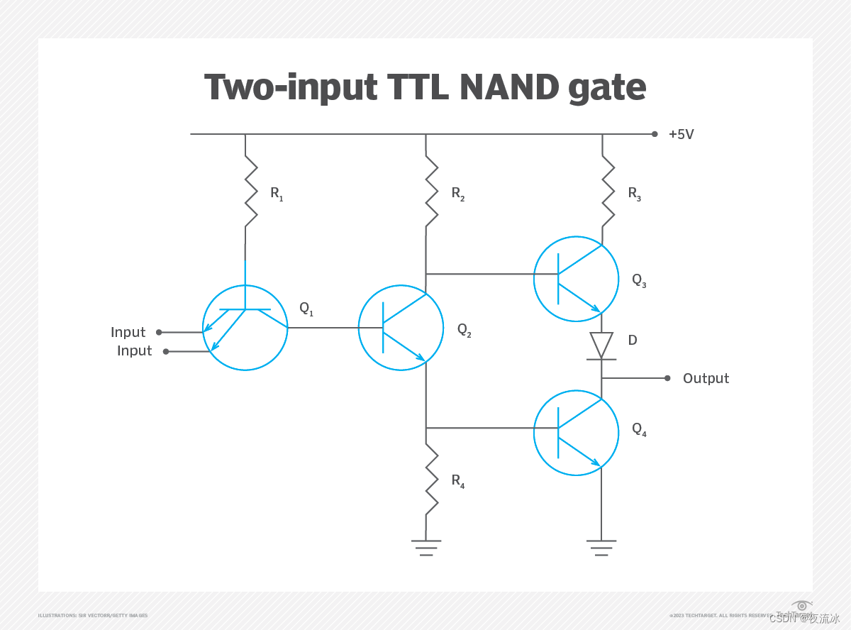
图 1. 该图显示了一个两输入 TTL NAND 栅极,其中有四个晶体管: Q1、Q2、Q3 和 Q4;四个电阻: R1、R2、R3 和 R4,以及一个二极管: Q1 是输入晶体管。Q2 起着分相器的作用。Q3 和 Q4 产生输出,为输出提供高扇出能力。
| Figure 1. This diagram shows a two-input TTL NAND gate with four transistors: Q1, Q2, Q3 and Q4; four resistors: R1, R2, R3 and R4; and a diode: D. Q1 is the input transistor. Q2 functions as a phase splitter. Q3 and Q4 create output that provides a high fan-out capability for the output. |
图 1 展示了一个基本的双输入 TTL NAND 栅极原理图。晶体管 Q1 是输入晶体管。A 和 B 等输入端为 Q1 的发射极供电。晶体管 Q2 充当分相器,晶体管 Q3 和 Q4 形成图腾柱输出,为输出提供高稳定性和高扇出能力。
| Figure 1 illustrates a basic two-input TTL NAND gate schematic. Transistor Q1 is the input transistor. Inputs, such as A and B, feed the emitter of Q1. Transistor Q2 serves as a phase splitter, and transistors Q3 and Q4 create a totem pole output that provides high stability and a high fan-out capability for the output. |
当输入端 A 和 B 开启(逻辑 1 或高电平)时,晶体管 Q2 和 Q3 接通并充当放大器,而晶体管 Q4 接通以产生逻辑 0 或低电平逻辑输出。当输入端 A 和 B 中的任何一个或两个处于关断状态(逻辑 0 或低电平)时,晶体管 Q2 和 Q4 关断,形成逻辑 1 或高电平逻辑输出。
| When inputs A and B are on -- logic 1 or high -- transistors Q2 and Q3 turn on and act as amplifiers, while transistor Q4 turns on to create a logic 0 or low logic output. When either or both inputs A and B are off -- logic 0 or low -- transistors Q2 and Q4 turn off to create a logic 1 or high logic output. |
该 NAND 门电路的逻辑表示如图 2 所示。
| The logical representation of this NAND gate circuit is shown in Figure 2. |
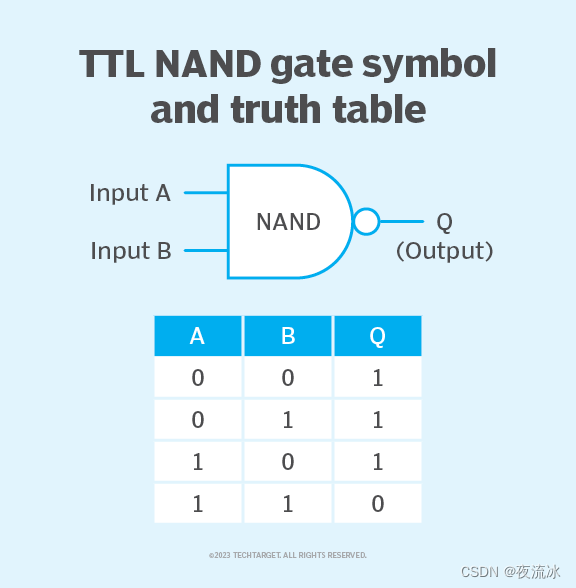
图 2. 基本双输入 TTL NAND 逻辑门的符号和真值表。
| Figure 2. Symbol and truth table for a basic two-input TTL NAND gate. |
其他逻辑门使用略有不同的电路配置来实现各自的逻辑行为,如 AND、OR 和 NOR,但总体概念是相似的。
| Other logic gates will use slightly different circuit configurations to achieve each respective logical behavior -- such as AND, OR and NOR -- but the overall concept is similar. |
Characteristics and considerations of TTL [ TTL 的特点和注意事项 ]
TTL 栅极电路和容纳栅极的集成电路封装涉及设计人员在数字电路设计中需要考虑的重要特性。虽然 TTL 元件在商业数字电路设计中已不再广泛使用,但其基本特性对于超大规模集成电路元件(如特定应用集成电路 (ASIC)、处理器和现代电子设备中使用的其他复杂数字元件)仍然非常重要。
| TTL gate circuits and the IC packages that hold the gates involve important characteristics that designers consider in their digital circuit designs. While TTL components are no longer widely used in commercial digital circuit design, the fundamental characteristics remain important for VLSI components, such as an application-specific integrated circuit (ASIC), processor and other complex digital components used in modern electronic devices. |
这些特性包括:
- 扇入。这是连接到栅极的输入数或 TTL 栅极可处理的输入数。
- 扇出。这是 TTL 栅极在不影响栅极性能的情况下可以驱动或操作的输出数量。这通常是来自其他 TTL 栅极的 10 个负载。
- 功率耗散。这是栅极或器件将消耗的功率。它是以伏特为单位的电源电压乘以以安培为单位的电流的乘积,通常以毫瓦(mW)为单位。典型 TTL 栅极的功率耗散约为 10 mW。
- 传播延迟。这是栅极输出响应栅极输入变化所需的时间。这是延迟的一种表现形式,它限制了整个数字电路的最高速度。传播延迟以纳秒(ns)为单位。典型 TTL 栅极的延迟约为 10 纳秒。
- 噪声裕量。数字信号并不完美;噪声裕量是指输入信号电压在不影响输出逻辑电平的情况下允许的电压范围。标准 TTL 栅极允许的噪声余量约为 0.4 伏。
- 温度范围。这是栅极允许的安全工作温度范围。标准 7400 系列 TTL 栅极的温度范围为 0 至 70 摄氏度;5400 系列栅极的温度范围扩大到负 55 至 125 摄氏度。
- 特殊特性。某些 TTL 栅极产品的制造具有高可靠性和抗辐射性,可用于军事和航空航天领域。
| These characteristics include the following: * Fan-in. This is the number of inputs connected to a gate or the number of inputs a TTL gate can handle. * Fan-out. This is the number of outputs a TTL gate can drive or operate without affecting the gate's performance. This is typically 10 loads from other TTL gates. * Power dissipation. This is the amount of power the gate or device will use. It's taken as the product of supply voltage, measured in volts, multiplied by the current drawn, measured in amperes, and is typically measured in milliwatts (mW). Power dissipation for a typical TTL gate is about 10 mW. * Propagation delay. This is the time needed for the gate's output to change in response to a change in the gate's inputs. This is an expression of latency, and it limits the overall digital circuit's top speed. Propagation delay is measured in nanoseconds (ns). The delay for a typical TTL gate is about 10 ns. * Noise margin. Digital signals aren't perfect; noise margin is the voltage range allowed for the input signal voltage that won't affect the output logic level. Standard TTL gates allow a noise margin of about 0.4 volts. * Temperature range. This is the range of safe operating temperatures allowed for the gate. Standard 7400 family TTL gates have a temperature range from 0 to 70 degrees Celsius; 5400 family gates have an extended range of minus 55 to 125 degrees Celsius. * Special characteristics. Some TTL gate products were fabricated for high reliability and radiation resistance for military and aerospace uses. |
Types of TTL
经过几十年的使用,TTL 电路设计不断发展和多样化,以优化某些特性,如速度、功耗和驱动其他元件的输出功率。最流行的 TTL 类型包括以下几种:
| TTL circuit designs evolved and diversified over decades of use to optimize certain characteristics such as speed, power consumption and output power to drive other components. The most popular types of TTL include the following: |
- 标准 TTL 代表传统的 7400 元件系列,具有标准特性,包括每个栅极 10 mW 的典型功耗和每个栅极 10 ns 的传播延迟。
- 快速 TTL 以更快的开关速度换取更高的功耗。例如,快速 TTL 栅极可能在 6 ns 内完成开关,但功耗为 22 mW。这有时被称为高功率 TTL。
- 低功耗 TTL 以较低的开关速度换取较低的功耗。例如,低功耗 TTL 栅极的功耗可能为 1 mW,但延迟可达 33 ns。
- 低压 TTL 使用 3.3 伏直流电压,而不是通常的 5 伏直流电压,因此每个栅极的功耗仅为 2 mW 左右。较低的电源电压将降低每个栅极的功耗,并有助于加快传播延迟,因为逻辑 0 和逻辑 1 电压电平的差异较小。
- 肖特基 TTL 包括 TTL 栅极中的肖特基二极管钳位,可将栅极开关时间加快到约 3 ns。不过,这会将每个栅极的功耗增加到约 19 mW。
- 低功耗肖特基 TTL 也称为高级肖特基 TTL,它结合了低功耗 TTL 和肖特基二极管,可提供 9.5 ns 的快速传播延迟,每个栅极的功耗为 2 mW。
- 集电极开路 TTL 使输出晶体管的集电极引线处于开路状态,实际上不需要芯片电源电压供电,因此设计人员可以将高电压或分组输出集成到芯片中,以驱动非 TTL 负载。集电极开路 TTL 集成电路的例子包括传统的 7401 和 7403。
- 三态 TTL,有时也称为三态 TTL,包括可使栅极断开的附加电路。它通常用于设计总线 TTL 电路,在这种电路中,同一根导线上可能存在多个栅极。第三个断开状态会产生一个高阻抗状态,隔离或断开栅极,防止其干扰使用公共总线连接的其他栅极。
| * Standard TTL represents the traditional 7400 family of components with standard characteristics, including a typical power dissipation of 10 mW per gate and a propagation delay of 10 ns per gate. * Fast TTL trades faster switching speeds for higher power consumption. For example, a fast TTL gate might switch in 6 ns but use 22 mW. This is sometimes called high-power TTL. * Low-power TTL trades lower power consumption for slower switching speeds. For example, a low-power TTL gate might use 1 mW but have a delay of up to 33 ns. * Low-voltage TTL uses a 3.3 volts direct current supply voltage instead of the usual 5 VDC supply voltage, resulting in only about 2 mW of power per gate. The lower supply voltage will lower power dissipation per gate and can help speed propagation delays because the difference in logic 0 and logic 1 voltage levels is smaller. * Schottky TTL includes Schottky diode clamps in the TTL gate, which accelerates gate switching time to about 3 ns. However, this increases power use to about 19 mW per gate. * Low-power Schottky TTL, also called advanced Schottky TTL, combines low-power TTL and Schottky diodes to offer a fast 9.5 ns propagation delay and 2 mW of power use per gate. * Open-collector TTL leaves the output transistor's collector lead open and effectively unpowered from the chip's supply voltage, allowing designers to incorporate high-voltage or grouped outputs to drive non-TTL loads. Examples of open-collector TTL ICs include the traditional 7401 and 7403. * Tri-state TTL, sometimes called three-state TTL, includes additional circuitry that lets the gate be disconnected. It's often used in the design of bus TTL circuitry where numerous gates might be present on the same wire. The third disconnected state creates a high-impedance state that isolates or disconnects the gate and prevents it from interfering with other gates using the common bus connections. |
Applications of TTL
从 20 世纪 60 年代到 80 年代,TTL出现后 一直是数字电子电路设计的标准。而在那之后,VLSI 和 ASIC 芯片等高度集成的定制数字元件的广泛采用取代了由门电路组成芯片。
TTL 因其低成本、稳定可靠的逻辑信号电平所需的稳固噪声裕量、可驱动后续 TTL 门的充足扇出以及可保持电路冷却和更节能的适度功率耗散等优势而广受欢迎。
| TTL was the standard for digital electronic circuit design from its inception in the 1960s through the 1980s. At that time, the broad adoption of highly integrated, custom-fabricated digital components such as VLSI and ASIC chips displaced the chips with individual gates. TTL was embraced for its advantages, such as low cost, solid noise margin for stable and reliable logic signal levels, ample fan-out to drive subsequent TTL gates, and modest power dissipation to keep circuits cooler and more energy-efficient. |
然而,TTL 的速度相对较慢,由许多栅极组成的电路非常耗电。尽管单个栅极的延迟时间只有几纳秒,但由于需要用许多栅极和芯片来构建大型复杂电路,传播延迟不断累积,从而限制了整个电路的最高速度。每个芯片中的门之间相互连接所需的印刷线路增加了延迟,并使大型电路容易受到电信号噪声的影响。因此,TTL 并不是高性能电路(如早期的处理器)的理想选择。
TTL 主要用于控制器类型的数字电路,包括简单的控制器、基本的计算机接口设计(如用于软盘和早期磁性硬盘驱动器的早期存储接口控制器)以及工业电子系统的专用电路。直到 TTL 逻辑门的逻辑功能被集成到 VLSI 和 ASIC 设备等高密度芯片中,数字电子产品才在商业和消费应用中大放异彩。
| However, TTL was relatively slow, and circuits composed of many gates were power-hungry. Even though individual gate delays measured just a few nanoseconds, the need to construct large, complex circuits from many gates and chips made the propagation delays cumulative, limiting the overall circuit's top speed. The printed wiring needed to interconnect the gates in each chip added to the latency and made large circuits vulnerable to electrical signal noise. As a result, TTL wasn't a good choice for high-performance circuits, such as early processors. TTL saw most of its service in controller-type digital circuits, including simple controllers, basic computer interface designs such as early storage interface controllers for floppy disks and early magnetic hard drives, and dedicated circuits for industrial electronic systems. It wasn't until the logic functions of TTL gates were integrated into high-density chips such as VLSI and ASIC devices that digital electronics exploded into commercial and consumer applications. |
TTL vs. emitter-coupled logic [ TTL 逻辑与射极耦合逻辑 ]
发射极耦合逻辑(ECL)是用于构建数字逻辑门的另一种电子电路设计。与 TTL 结构相比,ECL 结构使用过驱动双极晶体管差分放大器和有限的发射极电流,以防止晶体管饱和并完全导通。ECL 通常被称为电流转向逻辑,因为电流是在发射极耦合晶体管对之间转向的。
ECL 已成为引人注目的替代栅极设计;与 TTL 栅极设计相比,它的非饱和晶体管开关速度更快,传播延迟更低。ECL 栅极的典型传播延迟为 1 到 2 ns,而标准 TTL 栅极的传播延迟约为 10 ns。ECL 的扇出也更高,约为 25 个栅极负载,而 TTL 的扇出约为 10 个,这使得 ECL 栅极可以驱动更多的数字设备。
ECL 的主要缺点是功耗比 TTL 高得多。此外,逻辑 0 和逻辑 1 之间的低电压差使 ECL 栅极的抗噪能力较差。这两个因素限制了 ECL 电路的复杂性和使用案例。
TTL 为今天的逻辑门和数字电路奠定了基础。
| Emitter-coupled logic (ECL) is an alternative electronic circuit design used in the construction of digital logic gates. Compared with TTL construction, ECL construction uses an overdriven bipolar transistor differential amplifier and limited emitter current to prevent saturating the transistors and turning them fully on. ECL is often referred to as current-steering logic, because current is steered between the emitter-coupled transistor pair. ECL became a notable alternative gate design; its unsaturated transistors can be switched much faster, and with far lower propagation delay, than TTL gate designs. ECL gates demonstrate a typical propagation delay of 1 to 2 ns compared with about 10 ns for a standard TTL gate. ECL fan-out is also much higher at about 25 gate loads compared with a TTL fan-out of about 10, allowing ECL gates to drive more digital devices. The main disadvantage of ECL is its much higher power dissipation than TTL. In addition, the low voltage difference between logic 0 and logic 1 leaves ECL gates with poor noise immunity. These two factors limit ECL circuit complexity and use cases. TTL provided the foundation for today's logic gates and digital circuitry. |
参考:
1,Techtarget
What Is Transistor-to-Transistor Logic (TTL)? Definition from TechTarget